Cell Phone Signal Detector – Part 7, transmission line width… and KiCAD!
I made a couple of PCB versions of a cell phone signal detector and my board layout didn’t work as well as my evaluation board.

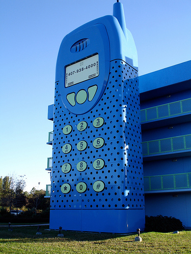
Thanks to Daryl Mitchell for the photo
For a long time, I thought it was because I was home-reflowing the QFN chip.
Recently, I had the opportunity to talk to people who do RF layout. It was then that I was introduced to the concept that a 4 layer board will require a much thinner transmission line (for a matched 50 ohms) than a 2 layer board.
My RF circuit requires 50 ohms for the best power transfer between the antenna and the rest of the circuit. You can read more about impedance matching on Wikipedia, but the basic idea here is when the antenna and the circuit have the same impedance, it is like a seamless wire. Ideally, you want your power source, transmission line and load to match, otherwise … it won’t work!
Unmatched impedances will cause your input signal to attenuate in power by varying degrees depending on how bad your impedance match is.
This concept is one of the first things I learned in Electromagnetics class in school, but there is no substitute for learning like hands-on!
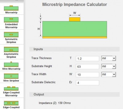
There are a number of transmission line calculators online. I chose the one from EE Web. I think it’s pretty clear from the diagram what the inputs mean, but just quick: the trace thickness is the thickness of your trace. You get this from the weight of your PCB. OSH Park, where I get my boards fabbed, has 1 oz copper on the top layer. My transmission line is on the top layer, which is 1 oz copper. Substrate height is the height between the bottom the trace to the next layer. Trace width is what controls the transmission line impedance, so you have to change this until your output reads the desired impedance. And the substrate dielectric is also available from your board house. It’s the Greek symbol εr and it means relative permittivity.

The width of my needed transmission line on a 4-layer board turned out to be 0.03mm. On a 2-layer board, the transmission line size needed is 3mm. I decided to go with a 4-layer board on my next round. My PCB layout software is a lite version of Eagle ($70), but Eagle doesn’t allow 4 layers with this version. I could pay $169 for a Hobbyist version which includes 6 signal layers, but I sell boards. The standard is $820, which is still an excellent price, considering many PCB software packages are thousands.
KiCAD is an open source, free software that allows multiple layers. For this circuit, it turned out to be an obvious choice. I learned enough of the software to make a board within 2 weeks, and
sent it off to be fabbed. I am impressed with how intuitive KiCAD is to learn, and will continue to use it on all of my boards that require more than 2 layers.
Link to part 6 in this series
Link to part 5 in this series
Link to part 4 in this series
Link to Diode Detector post
Link to part 3 in this series
Link to part 2 in this series
Link to part 1 in this series